A clean room in a microchip fabrication plant in Singapore.Credit: Lauryn Ishak/Bloomberg/Getty
One of the many consequences of the COVID-19 pandemic is a global shortage of the microchips that are essential to electronic devices. The factories that make these chips had to shut down for some of the pandemic, and are struggling to cope with an increase in demand. Some products could be delayed by months.
It’s too early to know how the shortage will affect the industry in the long term, but the pandemic has focused attention on some key research questions — including how to make the manufacturing process more resilient to shocks and emergencies.
One well-known problem is that microchips are designed in just a handful of companies, including Samsung in South Korea and Intel, NVIDIA and Qualcomm in California. But not all these companies make the chips. Some do; others outsource the work to third parties. And around 80% of the chips are made in Asia (Nature Electron. 4, 317; 2021). The biggest manufacturer is the Taiwan Semiconductor Manufacturing Company (TSMC) in Hsinchu, which is responsible for 28% of global capacity using current fabrication methods. Although this concentration has undoubtedly been of great benefit to the region, it has also contributed to the current restriction of supplies.
Signs of change are starting to emerge. China, the United States and some European countries are increasing investments in microchip research and development. Amazon, Google, Microsoft and other big US technology corporations are doing the same, with investments estimated at hundreds of millions of dollars. Spreading capability through more companies — and to more low- and middle-income countries — will help to make the industry more resilient.
Time-savers
Also of help is a report this week that researchers at Google have managed to greatly reduce the time needed to design microchips (A. Mirhoseini et al. Nature 594, 207–212; 2021). This is an important achievement and will be a huge help in speeding up the supply chain, but the technical expertise must be shared widely to make sure the ‘ecosystem’ of companies becomes genuinely global. And the industry must make sure that the time-saving techniques do not drive away people with the necessary core skills.
Read the paper: A graph placement methodology for fast chip design
Researchers and engineers continue to design and manufacture microchips with ever more processing power and complexity. In line with Moore’s law — the principle that the number of transistors per chip doubles roughly every two years as transistors become smaller (G. E. Moore Electronics 38, 114–117; 1965) — the number of transistors per microchip has increased from a few thousand in the early 1970s to tens of billions today.
Although fabrication of the chips is largely automated, the design still relies on manual processes. Engineers and designers use computer-aided design software, but it can still take them weeks or months to work out how to fit all the components into the available space. Google’s researchers have now shown that the process can be completed in less than a day by using artificial intelligence (AI).
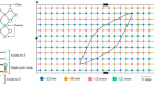
Typically, the area of a microchip is of the order of tens to hundreds of millimetres square. That space needs to accommodate thousands of components, such as memory, logic and processing units, plus many kilometres of ultra-thin wire to connect these components together. One of the most challenging aspects of the design process is ‘chip floorplanning’. This involves working out where best to place these components, in the same way that an architect designs a building’s internal space such that it can accommodate all the required fixtures and fittings.
AI system outperforms humans in designing floorplans for microchips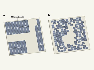
Google’s researchers used 10,000 chip floorplans to train their software. The software then worked out how to generate floorplans that used no more space, wire and electric power than did those designed by engineers. Miniaturization and low power are particularly important for the chips used in smartphones.
The AI-generated chips took less than six hours to design, and the method has already been used to design Google’s tensor processing unit, or TPU, which is used mainly in the company’s cloud-based machine-learning applications. More teams need to test the design software to make sure it is robust and can accommodate other data sets and chip types. If more groups can recreate its success, that will cement its place in the chip-design toolbox.
Now concentrate
More-accessible and more-efficient microchips will power the development of autonomous vehicles, 5G communications and AI — opportunities that should not be missed. But it’s important to consider the wider implications of using automated design technologies, particularly the need for people with relevant skills and expertise, and for upskilling those who currently do the process manually.
Chip floorplanning — whether manual or automated — requires expertise in computing, electronic engineering and device physics. These skills take time to learn and are sorely needed in an industry that makes many other products besides microchips. It’s crucial that the companies involved understand this, and take appropriate steps to meet their skills needs both locally and globally. Automation often fuels concerns about a reduction in jobs. In fact, maintaining momentum in the electronics industry will require people and companies with the foresight to create the next generation of microchips.
 Read the paper: A graph placement methodology for fast chip design
 AI system outperforms humans in designing floorplans for microchips
 Am I arguing with a machine? AI debaters highlight need for transparency
 Don’t ask if artificial intelligence is good or fair, ask how it shifts power
 Chips in a crisis
 The role of government policy in the building of a global semiconductor industry