


The ability of new blue-light semiconductor lasers to better perform precision cutting, patterning or welding of copper will make electrical and electronic component manufacturing cheaper and more sophisticated, says Hiroyuki Hagino, a research scientist for Panasonic, headquartered in Osaka, Japan.
Copper’s optical absorption of blue light is almost 10 times higher than for red and infrared light, he explains. The development of new blue semiconductor laser devices in Japan is building on an expertise in gallium-nitride semiconductor-based optical devices, used for LEDs. By tweaking the crystal layers of blue-light-producing wafers and the structure of waveguides, Panasonic researchers are on the path to developing new high-brightness lasers that could overcome some of the hurdles of processing copper, says Hagino.

These laser diodes use the semiconductor material indium gallium nitride to create blue light when pumped directly with electrical current. Copper absorbs blue light 10 times more than red and infrared light.
Ultimately, these laser systems should provide cheaper, more sophisticated electrical parts, particularly for the emerging electric vehicle industry, he adds.
CONTROLLING COPPER
Currently, manufacturing electrical components, including copper, is challenging. Copper is commonly used a space efficient material in electronic circuitry, because it’s relatively cheap and has high electrical conductivity.
But high electrical conductivity also means that copper has high thermal conductivity, which makes welding difficult. Any laser heat that is applied to a specific spot quickly transfers through to any other materials in contact with the copper. Zapping the metal with very high-power lasers could get around this issue, but copper absorbs little red or infrared light, where the highest power lasers operate.
Copper’s low absorption of red or infrared light also means that laser systems are highly sensitive to the condition of the metal’s surface, making reproducible results difficult. The same problem arises for other important metals used in electronics, such as gold.
But the emergence of blue-light lasers, which copper will absorb more readily, could help side-step these issues, says Hagino.
BLUE RIBBON LASERS
The history of the blue-light laser diode is closely linked to that of the blue LED. Early commercial semiconductor light sources were made using semiconductor compounds gallium arsenide or gallium phosphide, because they have excellent optical emission properties, and were fairly easy to produce as high-quality wafers.
But gallium arsenide and gallium phosphide naturally create infrared- or red-light. Chemically modifying the semiconductors allowed for a shift into the green part of the spectrum, but blue light remained elusive.
It wasn’t until the successful growth of gallium nitride semiconductor wafers in the 1990s that blue-light LEDs became possible. In fact, this development was seen as such a significant breakthrough that it won three Japanese researchers — Isamu Akasaki, Hiroshi Amano and Shuji Nakamura — the Nobel Prize in Physics in 2014.
WAFER THIN PRECISION
In addition to greater power, lasers for precision laser processing require a small laser spot size and long focus-depth. This has been achieved for infrared-light semiconductor lasers by fine turning light and waveguides. But this has yet to be fully realized with blue-light lasers, explains Hagino.
All lasers need a way of trapping or confining light, he explains. Semiconductor lasers achieve this using reflection at semiconductor-air surfaces or the interfaces between different semiconductor materials.
To achieve this reflection, thin semiconductor films are deposited on top of one another, and the laser beam is further defined by an etched channel through this stack. The thickness and composition of the layers, and the size and shape of the laser etching, can all be chosen to determine the laser’s properties and optimize the optical confinement.
The simplest channel structure is known as a ‘ridge waveguide’ — a long, thin rectangle, up to 50 micrometers in length and just one micrometer across, creating a strong optical confinement.
But producing a small spot size with blue light has been tricky, says Hiroshi Ohno, who manages the laser development team to which Hagino belongs. A high brightness laser beam requires both high emission power from the semiconductor and a high-quality beam, he explains. And in ridge-waveguide lasers, emission power and the quality of the beam are traded against one another, as increasing the width of the ridge produces a higher intensity output, but lowers beam quality.

Panasonic have already demonstrated an output power of 78 W with a high beam quality from a single laser array chip.
This happens because the wider laser supports numerous optical wave patterns, known as modes. “The more modes a laser supports, the more difficult it is to focus the beam of light on a smaller point,” explains Ohno.
So, they created a new indium gallium nitride laser with a novel lateral-corrugated waveguide, in which the long sides of the laser are etched into a zig-zag pattern, rather than being straight.
This architecture can selectively reduce higher wave modes and thus improves beam quality. In the proposed structure, the number of wave modes supported and scattered by their new waveguide is smaller than that of a conventional lateral-corrugated waveguide, which reduces quantum efficiency deterioration.
The team have already been able to demonstrate an output power of 78 W with a high beam quality (M2=3.5 on average) from a single laser array chip.
BEAM COMBINING
The next step for Panasonic is to combine the output of many such devices to attain the power required for laser cutting and drilling of more than 1 mm-thick copper – roughly 1 kilowatt.
To achieve this, they are incorporating another Panasonic-developed technology, known as wavelength beam combining, which uses an optical element to divide light into different wavelengths, allowing multiple laser beams to combine.
“We can fabricate an array of lasers on one chip and focus all the light together at one point,” explains Ohno.

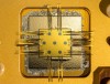
Panasonic have created a new blue-light indium gallium nitride laser (top) using a lateral-corrugated waveguide (bottom), which improves beam quality.
Panasonic had previously been able to create some of the world’s highest brightness blue lasers using wavelength beam combining. The team hope that, by marrying wavelength beam combining with their lateral-corrugated waveguide lasers, they might be able to achieve several hundred watts or even kilowatts with higher beam quality than ever before.
This would ideally be achieved by just a single wavelength beam combining system, which would bring into sight more compact blue-laser copper processing systems, adds Ohno.
Prototype machines based on these technologies are being used for application benchmarking at the Advanced Material Processing (AMP) Connect Lab in the Panasonic Group’s Toyonaka business division, or at the TACMI Consortium hosted by the University of Tokyo. Developed machines will quickly find use in Panasonic divisions that manufacture parts for electric cars, which will only grow as the market expands, says Hagino. “The electrical motors, batteries and fuel cells required for these vehicles all need precision laser processing,” he says.
 Focal Point on Emerging Photonic and Quantum Technologies in Japan