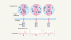
A neuromorphic chip, key to the predicted ‘paradigm shift’ in computing performance.Credit: Seung Hwan Lee
Solid-state computing has had a long run since the 1950s, when transistors began replacing vacuum tubes as the key component of electronic circuits. Generations of new solid-state devices that process and store information electronically at accelerated speeds came and went as germanium transistors were replaced by silicon transistors, followed by integrated circuits, then by increasingly complex chips filled with ever-higher counts of smaller transistors.
Since 1965, the industry has been guided by Moore’s law — predictions made by Gordon Moore, co-founder of microprocessor giant Intel — that ever-shrinking devices will lead to improved computing performance and energy efficiency. Advances in nanotechnology have allowed the smallest features on today’s most advanced integrated circuits to be shrunk to an atomic scale, but this is incompatible with current devices. The next major step in computing not only requires new nanomaterials — it needs a new architecture.
Nature Index 2022 Nanoscience and nanotechnology
CMOS (complementary metal-oxide-semiconductor) transistors have been the standard building blocks for integrated circuits since the 1980s. CMOS circuits, like generations of digital computers before them, rely on the fundamental architecture that John von Neumann chose in the mid-twentieth century. His architecture was designed to separate the electronics that store data in computers from those that process digital information. The computer stored information in one place, then sent it to other circuits for processing. Separating stored memory from the processor keeps the signals from interfering with each other and retains the accuracy needed for digital computing. However, the time spent moving data from memory to processors has become a bottleneck. Developers are now seeking alternative non-von Neumann architectures to perform calculations ‘within memory’ to avoid wasting time moving data around.
Another aim is to shift to neuromorphic systems, which use algorithms and network designs that emulate the high connectivity and parallel processing of the human brain. This means developing new artificial neurons and synapses that are compatible with electronic processing, but exceed the performance of CMOS circuits, says chemical and materials science researcher, Mark Hersam. It’s no small feat, he adds, but would be well worth the cost. “I’m more interested in neuromorphic computing than in-memory processing, since I believe that emulating the brain is a larger paradigm shift, with more potential upsides.”
The challenge, in both cases, is to identify the best technologies for the task, work that Hersam is pursuing at Northwestern University in Evanston, Illinois. In the Nature Index, which tracks articles in 82 selected natural-sciences journals, Northwestern University is placed second in the United States for nano-related output, after the Massachusetts Institute of Technology in Cambridge.
The first hints of a major change in computing emerged around 2012, as Moore’s law began to stall out and developers of deep learning — where systems improve their performance based on past experience — realized that general-purpose central processing units (CPUs) used in conventional computers could not meet their needs.
Towards faster processing
The strength of CPUs was their versatility, says Wilfried Haensch, who led a group developing concepts for computer memory at the IBM Watson Research Center in Yorktown Heights, New York, until his retirement in 2020. “Whatever program you come up with, the CPU can execute it,” says Haensch. “Whether it can execute it efficiently is a different story.”
Seeking better processors for deep learning, IBM developers turned to graphical processing units (GPUs), designed to perform advanced mathematics used for high-speed, three-dimensional imaging in computer games. IBM found that GPUs can run deep-learning algorithms much more efficiently than CPUs, so the team hard-wired chips to run particular processes.
“In other machines, you load data and instructions, but in data-flow machines, certain instructions are hard-wired in the processor, so you don’t have to load the instructions,” says Haensch. This marked a break from the conventional von Neumann model because data flowed through the hard-wired processor, as if operations were being performed in-memory. It also worked for the deep-learning algorithm, because about 80% of its operations used the same advanced mathematics as image processing.
Further fine-tuning of current materials only offers a short-term solution, says Haensch. There are many new ideas, new devices and new nanostructures, he says, but none is ready to replace CMOS. And there are no guarantees on whether, or when, they will be ready to deliver the transformation the industry needs.

Source: Nature Index
Among the most popular class of devices in development are memristors, which have both memory and electrical resistance. Memristors resemble standard electrical resistors, but applying an electrical input to them can alter their resistance, changing what’s stored in memory. With three layers — two terminals that connect to other devices, separated by a storage layer — their structure allows them to store data and process information. The concept was proposed in 1971, but it was not until 2007 that R. Stanley Williams, a research scientist at Hewlett-Packard Labs in Palo Alto, California, made the first thin-film solid-state memristor that was usable in a circuit.
Memristors can be made on a nanometre scale and can switch in less than a nanosecond. They have “great potential for developing future computing systems past the von Neumann and Moore’s law eras”, Wei Lu and his group at the University of Michigan in Ann Arbor outlined in a 2018 review of memristor technology (M. A. Zidan et al. Nature Electron. 1, 22–29; 2018). Building a single system that combines all of the desired properties will not be easy.
Next-generation materials
Researchers are looking to new classes of materials to meet the needs of advanced computing. Hersam and his colleague Vinod K. Sangwan, a materials science and engineering researcher at Northwestern University, have catalogued an extensive list of potential neuromorphic electronic materials that includes zero-dimensional materials (quantum dots), one-dimensional and two-dimensional materials (graphene), and van der Waals heterostructures (multiple two-dimensional layers of materials that adhere together) (V. K. Sangwan and M. C. Hersam Nature Nanotechnol. 15, 517–528; 2020).
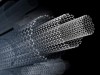
One-dimensional carbon nanotubes, for example, have attracted attention for their use in neuromorphic systems because they resemble the tubular axons through which nerve cells transmit electric signals in biological systems.
Opinions are divided on how these materials will factor into the future of computing. Abu Sebastian, the Zurich-based technical leader of the IBM Research AI Hardware Center in Albany, New York, is focused on near-term gains, and sees opportunities to push further in both digital and neuromorphic computing.
“Companies such as Mythic [an artificial intelligence company based in Austin, Texas] are very close to commercialization,” he says. On the research side, Lu says there’s a lot to figure out. The complex computations adapted from imaging need to be made “tighter and more accurate” for neuromorphic computing to take full advantage, he says. Haensch adds that there is so far no material to enable viable commercial production.
Intel and IBM, which is the leading corporate institution for nanoscience and nanotechnology-related output in the Nature Index, have large groups working on non-von Neumann computing. Hewlett-Packard and Paris-based artificial intelligence firm Lights-On are among several companies that are focused on near-term applications.
 The nanoscience revolution
 How cross-border collaboration underpins the nanoscience revolution
 Four rising stars who are reshaping nanoscience
 Why I wrote a children’s book about nanoscience
 Improving crop resilience with nanoparticles
 Teamwork drives Australia’s success in nanoscience