Abstract
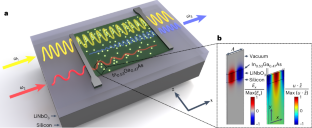
Efficient and deterministic nonlinear phononic interactions could revolutionize classical and quantum information processing at radio frequencies in much the same way that nonlinear photonic interactions have at optical frequencies. Here we show that in the important class of phononic materials that are piezoelectric, deterministic nonlinear phononic interactions can be enhanced by orders of magnitude via the heterogeneous integration of high-mobility semiconductor materials. To this end, a lithium niobate and indium gallium arsenide heterostructure is utilized to produce the most efficient three- and four-wave phononic mixing to date, to the best of our knowledge. We then show that the conversion efficiency can be further enhanced by applying semiconductor bias fields that amplify the phonons. We present a theoretical model that accurately predicts the three-wave mixing efficiencies in this work and extrapolate that these nonlinearities can be enhanced far beyond what is demonstrated here by confining phonons to smaller dimensions in waveguides and optimizing the semiconductor material properties.
This is a preview of subscription content, access via your institution
Access options
Access Nature and 54 other Nature Portfolio journals
Get Nature+, our best-value online-access subscription
$29.99 / 30 days
cancel any time
Subscribe to this journal
Receive 12 print issues and online access
$259.00 per year
only $21.58 per issue
Buy this article
- Purchase on Springer Link
- Instant access to full article PDF
Prices may be subject to local taxes which are calculated during checkout


Data availability
The data that support the findings of this study are available from the corresponding author upon reasonable request.
References
Hendrickson, S. M., Foster, A. C., Camacho, R. M. & Clader, B. D. Integrated nonlinear photonics: emerging applications and ongoing challenges. J. Opt. Soc. Am. B 31, 3193–3203 (2014).
Leuthold, J., Koos, C. & Freude, W. Nonlinear silicon photonics. Nat. Photon. 4, 535–544 (2010).
Moody, G., Chang, L., Steiner, T. J. & Bowers, J. E. Chip-scale nonlinear photonics for quantum light generation. AVS Quantum Sci. 2, 041702 (2020).
Bers, A. & Cafarella, J. Surface state memory in surface acoustoelectric correlator. Appl. Phys. Lett. 25, 133–135 (1974).
Cafarella, J. H., Brown, W., Stern, E. & Alusow, J. Acoustoelectric convolvers for programmable matched filtering in spread-spectrum systems. Proc. IEEE 64, 756–759 (1976).
Kino, G. S. Acoustoelectric interactions in acoustic-surface-wave devices. Proc. IEEE 64, 724–748 (1976).
Reible, S. A. Acoustoelectric convolver technology for spread-spectrum communications. IEEE Trans. Microw. Theory Techn. 29, 463–474 (1981).
Hackett, L. et al. Towards single-chip radiofrequency signal processing via acoustoelectric electron–phonon interactions. Nat. Commun. 12, 2769 (2021).
Bogdanov, S., Shalaginov, M., Boltasseva, A. & Shalaev, V. M. Material platforms for integrated quantum photonics. Opt. Mater. Express 7, 111–132 (2017).
Elshaari, A. W., Pernice, W., Srinivasan, K., Benson, O. & Zwiller, V. Hybrid integrated quantum photonic circuits. Nat. Photon. 14, 285–298 (2020).
Politi, A., Matthews, J. C., Thompson, M. G. & O’Brien, J. L. Integrated quantum photonics. IEEE J. Sel. Topics Quantum Electron. 15, 1673–1684 (2009).
MacCabe, G. S. et al. Nano-acoustic resonator with ultralong phonon lifetime. Science 370, 840–843 (2020).
Wollack, E. A. et al. Loss channels affecting lithium niobate phononic crystal resonators at cryogenic temperature. Appl. Phys. Lett. 118, 123501 (2021).
Guo, Y. & Wang, M. Phonon hydrodynamics and its applications in nanoscale heat transport. Phys. Rep. 595, 1–44 (2015).
Joshi, A. & Majumdar, A. Transient ballistic and diffusive phonon heat transport in thin films. J. Appl. Phys. 74, 31–39 (1993).
Arora, V. K. & Naeem, A. Phonon-scattering-limited mobility in a quantum-well heterostructure. Phys. Rev. B 31, 3887 (1985).
Hwang, E. & Sarma, S. D. Acoustic phonon scattering limited carrier mobility in two-dimensional extrinsic graphene. Phys. Rev. B 77, 115449 (2008).
Zhou, J.-J. & Bernardi, M. Ab initio electron mobility and polar phonon scattering in GaAs. Phys. Rev. B 94, 201201 (2016).
Shao, L. et al. Electrical control of surface acoustic waves. Nat. Electron. 5, 348–355 (2022).
Abdelkefi, A., Nayfeh, A. H. & Hajj, M. R. Effects of nonlinear piezoelectric coupling on energy harvesters under direct excitation. Nonlinear Dyn. 67, 1221–1232 (2012).
Mahboob, I., Wilmart, Q., Nishiguchi, K., Fujiwara, A. & Yamaguchi, H. Wide-band idler generation in a GaAs electromechanical resonator. Phys. Rev. B 84, 113411 (2011).
Luukkala, M. V. & Kino, G. Convolution and time inversion using parametric interactions of acoustic surface waves. Appl. Phys. Lett. 18, 393–394 (1971).
Kurosu, M., Hatanaka, D., Onomitsu, K. & Yamaguchi, H. On-chip temporal focusing of elastic waves in a phononic crystal waveguide. Nat. Commun. 9, 1331 (2018).
Kurosu, M., Hatanaka, D. & Yamaguchi, H. Mechanical Kerr nonlinearity of wave propagation in an on-chip nanoelectromechanical waveguide. Phys. Rev. Appl. 13, 014056 (2020).
Maksymov, I. S., Huy Nguyen, B. Q., Pototsky, A. & Suslov, S. Acoustic, phononic, Brillouin light scattering and Faraday wave-based frequency combs: physical foundations and applications. Sensors 22, 3921 (2022).
Mansoorzare, H. & Abdolvand, R. Acoustoelectric-driven frequency mixing in micromachined lithium niobate on silicon waveguides. In 2023 IEEE 36th International Conference on Micro Electro Mechanical Systems (MEMS) 1183–1185 (IEEE, 2023).
Mayor, F. M. et al. Gigahertz phononic integrated circuits on thin-film lithium niobate on sapphire. Phys. Rev. Appl. 15, 014039 (2021).
Coldren, L. A. & Kino, G. Monolithic acoustic surface‐wave amplifier. Appl. Phys. Lett. 18, 317–319 (1971).
Hackett, L. et al. Non-reciprocal acoustoelectric microwave amplifiers with net gain and low noise in continuous operation. Nat. Electron. 6, 76–85 (2023).
Mansoorzare, H. & Abdolvand, R. Micromachined heterostructured Lamb mode waveguides for acoustoelectric signal processing. IEEE Trans. Microw. Theory Techn. 70, 5195–5204 (2022).
Eichenfield, M. & Olsson, R. Design, fabrication, and measurement of RF IDTs for efficient coupling to wavelength-scale structures in thin piezoelectric films. In 2013 IEEE International Ultrasonics Symposium (IUS) 753–756 (IEEE, 2013).
Kumar, P. Quantum frequency conversion. Opt. Lett. 15, 1476–1478 (1990).
Mirhosseini, M., Sipahigil, A., Kalaee, M. & Painter, O. Superconducting qubit to optical photon transduction. Nature 588, 599–603 (2020).
Jiang, W. et al. Efficient bidirectional piezo-optomechanical transduction between microwave and optical frequency. Nat. Commun. 11, 1166 (2020).
Banszerus, L. et al. Ultrahigh-mobility graphene devices from chemical vapor deposition on reusable copper. Sci. Adv. 1, e1500222 (2015).
Kim, M.-S. et al. Sheet resistance analysis of interface-engineered multilayer graphene: mobility versus sheet carrier concentration. ACS Appl. Mater. Interfaces 12, 30932–30940 (2020).
Laroche, D., Das Sarma, S., Gervais, G., Lilly, M. & Reno, J. Scattering mechanism in modulation-doped shallow two-dimensional electron gases. Appl. Phys. Lett. 96, 162112 (2010).
Acknowledgements
This material is based on research sponsored in part by the Defense Advanced Research Projects Agency (DARPA) through a Young Faculty Award (YFA) under grant D23AP00174-00. The views and conclusions contained herein are those of the authors and should not be interpreted as necessarily representing the official policies or endorsements, either expressed or implied, by DARPA, the Department of the Interior, or the US Government. This work is supported by the Laboratory Directed Research and Development program at Sandia National Laboratories, a multimission laboratory managed and operated by National Technology and Engineering Solutions of Sandia LLC, a wholly owned subsidiary of Honeywell International Inc. for the US Department of Energy’s National Nuclear Security Administration under contract DE-NA0003525. This work was performed, in part, at the Center for Integrated Nanotechnologies, an Office of Science User Facility, operated for the US Department of Energy Office of Science. This paper describes objective technical results and analysis. Any subjective views or opinions that might be expressed in the paper do not necessarily represent the views of the US Department of Energy or the US Government.
Author information
Authors and Affiliations
Contributions
L.H. and M.E. came up with the device concepts and experimental implementations. M.E. developed the LDV system. M.K. performed the measurements with the LDV system with input from L.H., N.O. and M.E.. L.H., B.S., M.M., S.W., S.A., T.A.F. and M.E. designed the devices and fabrication process flow. M.M., S.W., B.S. and S.A. fabricated the devices. L.H., M.K., B.S. and S.S. performed the measurements. L.H. and M.E. carried out all of the modelling. L.H., M.K. and M.E. analysed all data with input from N.O. The manuscript was written by L.H., M.K. and M.E. and all authors have given approval for the final version.
Corresponding author
Ethics declarations
Competing interests
The authors declare no competing interests.
Peer review
Peer review information
Nature Materials thanks Linbo Shao and the other, anonymous, reviewer(s) for their contribution to the peer review of this work.
Additional information
Publisher’s note Springer Nature remains neutral with regard to jurisdictional claims in published maps and institutional affiliations.
Supplementary information
Supplementary Information
Supplementary Notes 1–8.
Rights and permissions
Springer Nature or its licensor (e.g. a society or other partner) holds exclusive rights to this article under a publishing agreement with the author(s) or other rightsholder(s); author self-archiving of the accepted manuscript version of this article is solely governed by the terms of such publishing agreement and applicable law.
About this article
Cite this article
Hackett, L., Koppa, M., Smith, B. et al. Giant electron-mediated phononic nonlinearity in semiconductor–piezoelectric heterostructures. Nat. Mater. (2024). https://doi.org/10.1038/s41563-024-01882-4
Received:
Accepted:
Published:
DOI: https://doi.org/10.1038/s41563-024-01882-4


